kelvin probe technology
Scanning Kelvin Probe (SKP)
|
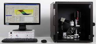
Scanning Kelvin Probes gives the user full access to 2D and 3D Work Function plots of samples ranging in size from 50 mm to 350 mm. With work function resolution of 1 - 3 meV, and the spatial resolution of the probe tip diameter.
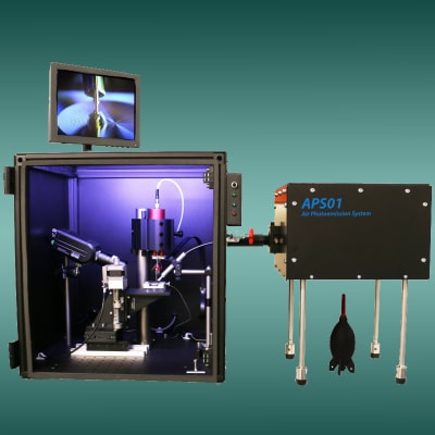
The Scanning Kelvin Probe is capable of reproducing reliable measurements for work function, contact potential difference and Volta potential. It is the perfect support for Ambient Pressure Photoemission Spectroscopy and Surface Photovoltage modules. |
SPECIFICATIONS
Tip material / Diameter Standard 2 mm gold tip (0.05 mm available on request) Work Function Resolution 1 - 3 meV Sample Scan Size 50 x 50 mm, 100 x 100 mm, 200 x 250 mm, 350 x 350 mm Height Control (auto) 25 mm/50 mm |
Single Point Kelvin Probe (KP)
|
Our Single-Point Kelvin Probe systems are the introductory systems to the Kelvin Probe range. The off-null signal detection method allows very high-quality measurements of the work function/Fermi level of materials.
A mini version is also available with a 55% smaller footprint in our 300 x 300 mm optical enclosure. |
SPECIFICATIONS
Tip material / Diameter Standard 2 mm gold tip (other sizes & materials available on request) Work Function Resolution 1 - 3 meV Probe Translation 25 mm manual translation Faraday / Optical enclosure 450 mm x 450 mm 300 mm x 300 mm (mini version) |
RELATIVE HUMIDITY/CORROSION KELVIN PROBE (RHC)
|
The Relative Humidity Kelvin Probe (RHC) systems are the ideal solution for monitoring samples in a controlled atmosphere for contact potential difference (CPD)/work function (Φ) measurements.
The RHC systems can automatically control the relative humidity within the chamber from 20% to 85% using the easily programmable software. |
SPECIFICATIONS
Tip material / Diameter 2 mm stainless steel tip Work Function Resolution 1 - 3 meV Sample Scanning* Single-point/50 x 50 mm Relative Humidity Control Automatic 20 - 80% Atmospheric Control* RH only / Oxygen <1% Breadboard Footprint 900 x 600 mm *Depending on model |
Surface Photovoltage (SPV) & SURFACE PHOTOVOLTAGE SPECTROSCOPY (SPS)
|
The surface photovoltage spectroscopy modules are the perfect all-in-one solution for in-depth studies of light-sensitive materials such as organic semiconductors, solar cells or light-sensitive dyes.
The modules offer a comprehensive range of measurement modes, including DC and AC surface photovoltage studies utilising the built-in optical chopper. The surface photovoltage technique is a simple and powerful tool for researching semiconductors, particularly for studying interfaces with defects as the technique allows light-induced surface potential to be measured too. |
SPECIFICATIONS
Wavelength 400 to 700 nm range 400 to 1000 nm range Intense white light QTH source DC and AC measurement modes Compatible with all Kelvin probe systems |
Ultra High Vacuum Kelvin Probe (UHV)
|
Ultra-high Vacuum Kelvin Probes gives the user full access to work function and contact potential difference (CPD) measurements under vacuum.
Each system comes with a high quality manual or motorised translator, allowing reliable and accurate tip-to-sample positioning, and the unrivalled tracking system holds the tip separation constant at all times during the measurement. The UHV produces a work function resolution is 1 - 3 meV, even under pressure |
SPECIFICATIONS
Tip material / Diameter 4 mm - 10 mm stainless steel tip (other diameters available) Work Function Resolution 1 - 3 meV Standard Translator 50 mm manual translator Motorised Translator Sizes 50 mm or 100 mm manual or motorised translators Height Control (Auto) Approximately 1 - 5 mm by DC offset (unless motorised) |
Ultra-high Vacuum Ф4 Kelvin Probe
|
The Ф4 Ultra-high Vacuum Scanning Kelvin Probe system gives the user full access to work function measurements under vacuum with the ability to alter the temperature from 77 K to 860 K . The system can be upgraded with surface photovoltage spectroscopy through utilising other ports in the system chamber.
Liquid nitrogen is used as the method of cooling the sample and heating is achieved by controllable direct current. Nitrogen gas is used to displace the oxygen to facilitate the use of the photoemission system source. An optical breadboard is used to support the chamber and standard power is required for operation. |
SPECIFICATIONS
Tip material / Diameter 2 mm/4 mm/10 mm stainless steel tip Work Function Resolution 1 - 3 meV Manual Translation 100 mm manual translator Scan Control Automatic via user interface (20 x 20 mm) Energy Range (APS / SPS) 3.4 - 7.0 eV / 1.24 - 3.10 eV Vacuum Compatibility 1 x 10⁻⁹ mBar |
Related instruments
|
*Pictures shown above are for reference only. Actual product may differ slightly.
*Some products may not be available in all countries. Please contact us for further information and clarification. |
Don't have what you are looking for?
Search here. Alternatively, please contact us for more information.
|


