
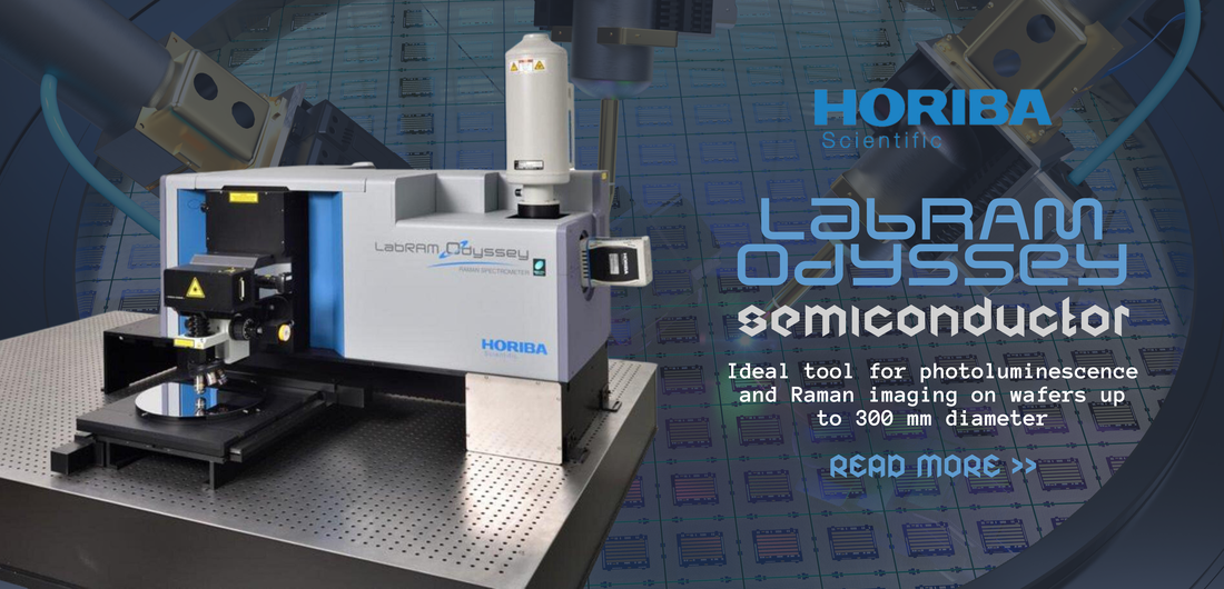
 HORIBA is pleased to introduce the latest addition to its repertoire, the LabRAM Odyssey Semiconductor system. This pioneering Raman/Photoluminescence microscope derives its foundation from the widely acclaimed LabRAM HR Evolution Confocal Raman Microscope, renowned for its exceptional high resolution capabilities. Noteworthy enhancements include the integration of a sample mounting stage adept at accommodating the prevalent 300 mm wafer size, catering directly to the semiconductor industry's standard requirements. As compound semiconductors are becoming more complex with a higher number of elements, uniformity assessment on blanket wafers is essential for high quality devices and high yield. The LabRAM Odyssey Semiconductor system will help process engineers qualify the different process steps in a timely manner and with a high level of confidence. With a high spatial resolution mode, the LabRAM Odyssey Semiconductor offers the capability to detect and identify defects and submicron inhomogeneities to understand and give insights about their origin.
The LabRAM Odyssey Semiconductor system includes a 300 mm × 300 mm automated sample stage and an automated objective turret, enabling the acquisition of maps of full wafers of diameter up of 300 mm. In addition, the DuoScan imaging function permits both variable size laser macrospot for full wafer maps and high spatial submicron step scanning for small area maps. The range of available excitation lasers, combined with a wide range of spectral detection, from deep UV to near IR, makes the LabRAM Odyssey Semiconductor system a two-in-one Raman and Photoluminescence spectroscopy tool. The “Tilt at midway” autofocus function overcomes possible sample/holder tilt and ensures reliability in uniformity response. As Raman and Photoluminescence characterization is moving from the lab to the fab for the emerging 2D materials-based devices, the LabRAM Odyssey Semiconductor system is the perfect tool for metrology technical managers.
0 Comments
Leave a Reply. |
HappeningsBesides keeping all informed about our current activities,we will also be showcasing some of our customers' works and research updates on this page.
Archives
October 2023
Categories
All
|
 RSS Feed