
Low-dimensional material transfer platform
We provide a wide selection of high-stability, high-precision mechanical design and high-quality microscopic imaging system enable precise transfer of tiny samples less than 5 μm.
multifunctional high-precision 2D material transfer system
Commercial solutions for low-dimensional material heterojunction device transfer
The multifunctional high-precision 2D material transfer system is a commercial solution for the transfer of low-dimensional material heterojunction devices.
The multifunctional high-precision 2D material transfer system is composed of a microscopy system, a three-axis transfer stage & a vacuum sample stage with heating. The stage can be rotated manually/motorised through a large angle. It is a powerful tool for analysing the effects of magic angle superconductivity, spatial inversion symmetry breaking in heterojunction, and different stacking methods of 2D materials. |
FEATURES
Microscopic imaging light path system
Coaxial illumination system 20X objective lens Zoom ratio: 1:6.5 Zoom range: 0.7X-4.5X Standard working distance: 90mm Resolution: 63-180lp/mm Comprehensive maximum magnification: 850~900 times CMOS microscope camera Comprehensive magnification up to 3500 x Transfer sample stage XYR three-axis adjustable XY direction range: 20mm System resolution: 0.002mm Manual adjustment rotation: ~ z- axis ± 90° Micrometer fine adjustment range: 5° Adjustment accuracy: 1° Max heating temperature: 260 ℃ Flow rate of the vacuum pump: 50L/min Slide platform XYZ three-axis adjustable 80 mm high-stability stainless steel table XY-axis travel: 25mm Z- axis: 29mm high precision micrometer Stage diameter: 100mm Coarse Adjustment Rotation Range: 360° Fine adjustment rotation range: ± 5° Positioning accuracy: 1~ 2° |
Motorised 2D material transfer system
Motorised Z-axis for low-dimensional material transfer system
This 2D material transfer system is a motorised version of the original multifunctional high-precision 2D material transfer system. With the motorised Z axis stage, coupled with the manual operation of the glass slide moving platform; users can achieve the slow bonding of the heterojunction interface while reducing the bubbles defects & other problems caused during the transfer process.
The 2D material transfer system is suitable for precise transfer of single-layer materials such as graphene, molybdenum disulphide, black phosphorus, and the preparation of multilayer van der Waals heterojunctions. The transfer system is composed of a microscopy system, a three-axis transfer stage, and a vacuum stage with heating. The stage can be rotated manually/motorised through a large angle. It is a powerful tool for analysing the effects of magic angle superconductivity, spatial inversion symmetry breaking in heterojunction, and different stacking methods of 2D materials. |
FEATURES
Motorised Z-axis
Travel Range: 25mm Minimum Travel Range Accuracy: 0.5um Motor and controller Motorised Rotation Rotatable Range: ± 90 ° Accuracy: 0.1° Continuous & single-step rotation function Imaging System Continuously adjustable zoom Coaxial with 20X long working distance objective Resolution: 1200 million pixels USB3.0 ultra high-definition CMOS Microscopy cameras Substrate Loading Platform XY Travel Range: 13mm Horizontal tilt angle: 3~5 ° Micrometer fine adjustment range: 5° Max heating temperature: 150 ℃ Vacuum sample stage with heating Solenoid valve controlled vacuum pump Flow rate of the vacuum pump: 50L/min Sliding Platform XY Travel Range: 25mm |
diamond anvil 2D-material transfer system
2d material regular transfer & diamond to anvil transfer simultaneously
The diamond anvil 2D-material transfer system is a commercial solution for the transfer of low-dimensional material heterojunction devices. It is suitable for precise point transfer of single-layer materials such as graphene, molybdenum disulphide, and black phosphorus, as well as multilayer van der Waals, achieving the preparation of the visual operation for low-dimensional material transfer.
The diamond anvil 2D-material transfer system is a special design for the fixture of the slide moving platform and the sample stage of the substrate loading platform on the basis of multifunctional high-precision 2D material transfer system. The diamond anvil 2D-material transfer system can simultaneously meet the conventional transfer of 2D materials and the transfer to DAC (Diamond Anvil Cell), further satisfying the preparation of 2D material under high-pressure conditions. The multifunctional high-precision 2D material transfer system is composed of a microscopy system, a three-axis transfer stage & a vacuum sample stage with heating. |
FEATURES
Imaging Optical
Continuously adjustable zoom Coaxial, with 20 times the long working distance objective lens Resolution: 1920 x 1080 High-definition CMOS Microscopy cameras Substrate Loading platform XY direction travel range: 13mm Horizontal tilt angle: 3~5 ° Manual adjustment rotation: ~ z- axis ± 90° Max heating temperature: 240 ℃ Vacuum sample stage with heating Solenoid valve controlled vacuum pump Flow rate of the vacuum pump: 50L/min Sliding platform Travel in the XYZ direction Travel Range: 25mm Accuracy: 0.001mm *The E1-S system does not contain a DAC device, & the sample stage is customisable according to customer's DAC size
|
2D material metallographic microtransfer system
High-definition imaging, eyepiece observation, can integrate Raman, fluorescence spectrum test, transfer simultaneous test
E1-M is suitable for precise point transfer of single-layer materials such as graphene, molybdenum disulphide, and black phosphorus, as well as the preparation of multilayer van der Waals heterojunctions, achieving visualisation of low-dimensional material transfer.
On the basis of retaining the excellent transfer integration operation of E1-T, E1-M has greatly improved the resolution and clarity of single-layer, multi-layer and various van der Waals heterojunction observations by upgrading the optical system of the metallographic microscope. The transfer system is composed of a microscopy system, a three-axis transfer table, and a a vacuum sample stage with heating. The target substrate stage can be rotated through large angle in the plane. |
FEATURES
Imaging Optical
Trinocular tube: 5 ,10, 20, 50 -fold 12-megapixel USB3.0 ultra-high-definition CMOS SubStation 4 subsystems: Substrate loading platform adjustment subsystem Slide moving platform adjustment subsystem Microscopic imaging subsystem Circuit control subsystem Slide Glass Adjustable in XYZ three-axis XY travel range: 25mm Coarse Adjustment Rotation Range: 360° Fine adjustment rotation range: ± 5° Positioning accuracy: 1~ 2° Sample Stage Linear movement through the steel ball gapless guide rail Adjustable XYZ axis Travel Range: 20mm Resolution: 0.002mm Manual adjustment rotation: ~ z- axis ± 90° Tilt around the x-axis and y-axis: ±3° |
2D MATERIAL VACUUM TRANSFER SYSTEM
2D material vacuum transfer system
In the process of preparing a 2D semiconductor material transistor with a multilayer heterojunction structure, it is necessary to transfer one layer of 2D material to another layer of 2D material.
Scientist often faced with two significant problems during multilayer material transfer. Firstly, when the transfer operation is performed under atmospheric environment, it is inevitable to result in air bubbles formation between the two layers of materials. Secondly, some 2D materials are sensitive to moisture and oxygen, which would significantly reduce the performance of the material itself. Both of these problems cause the device performance to decrease significantly. The 2D material vacuum transfer systems is capable of mitigating these two issues by integrating the system with; ultra-low vacuum environment, ultra-long working distance objective lens, full motorisation, high-precision micro-manipulation module, in-situ high-precision heating / cooling module & other components to achieve material transfer process under vacuum conditions. |
FEATURES
4-axis adjustable substrate loading platform
X/Y 2-axis motorised adjustable displacement sliding table Travel Range: 13mm Positioning Accuracy: 0.2 μm Max Speed: 350 μm/s Min Speed: 2 μm/s Motorised Rotary Table around Z-axis Max Speed: ± 20°/s Min Speed: ± 0.1°/s Positioning Accuracy: 0.1° Rotatable Range: ± 90 ° Loading Platform Highest heating temperature: 150 ℃ Lowest temperature: 10 ℃ Heating Rate: up to 2 ℃ /s Cooling Rate: up to 1.5 ℃ /s Deviation: <0.03 ℃ 4-axis adjustable slide moving platform X/Y 2-axis motorised adjustable displacement sliding table Travel Range: 25mm Positioning Accuracy: 0.2 μm Max Speed: 350 μm/s Min Speed: 2 μm/s Motorised Lifting Sliding Stage Travel Range: 10 mm Positioning Accuracy: 0.2 μm Max Speed of motorised displacement: 200 μm/s Min Speed: 5 μm/s *multiple speeds is available Motorised microscope focusing Z axis Motorised Z-axis lift slide Travel Range: 10mm Positioning Accuracy: 0.2 μm Speed of Motorised Displacement Max: 350 μm / S Min: 10 μm/s |
Related products
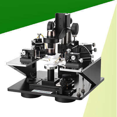
Probe Stations
|
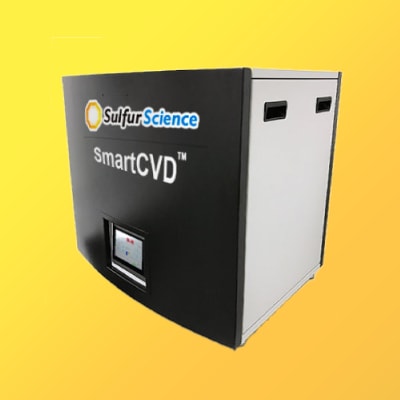
Chemical Vapour Deposition (CVD)
|
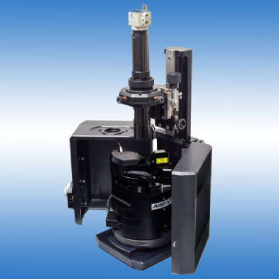
Atomic Force Microscope (AFM)
|
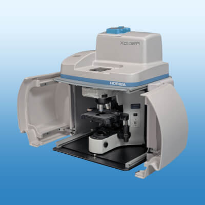
Raman Spectroscopy
|
|
*Pictures shown above are for reference only. Actual product may differ slightly.
**Some products may not be available in all countries. Please contact us for further information and clarification. |
Don't have what you are looking for?
Search Here. Alternatively, please contact us for more information.
|